目录
引言
知识储备
实际操作
设计源码
仿真源码
VCS执行仿真
DC 综合

引言
本篇继续学习 DC的基本使用。本篇主要学习 DC 综合之后的效果分析,重点在时序分析。
前文链接:
Design Compiler工具学习笔记(1)
Design Compiler工具学习笔记(2)
Design Compiler工具学习笔记(3)
Design Compiler工具学习笔记(4)
Design Compiler工具学习笔记(5)
知识储备
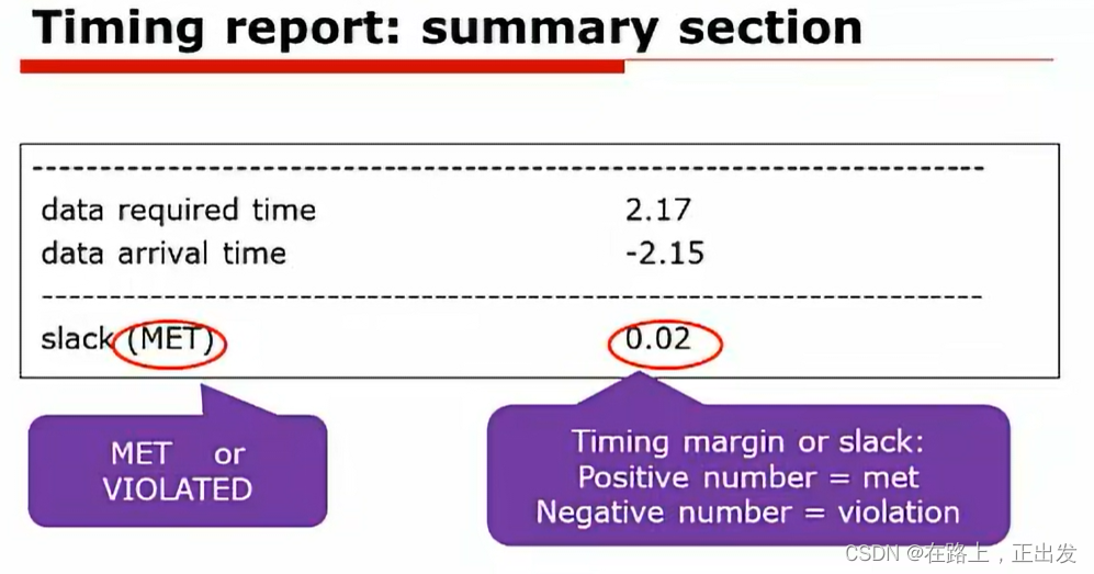
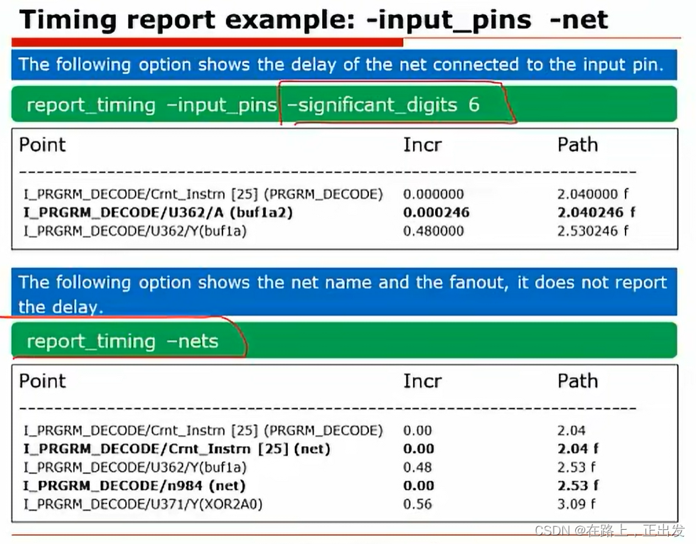
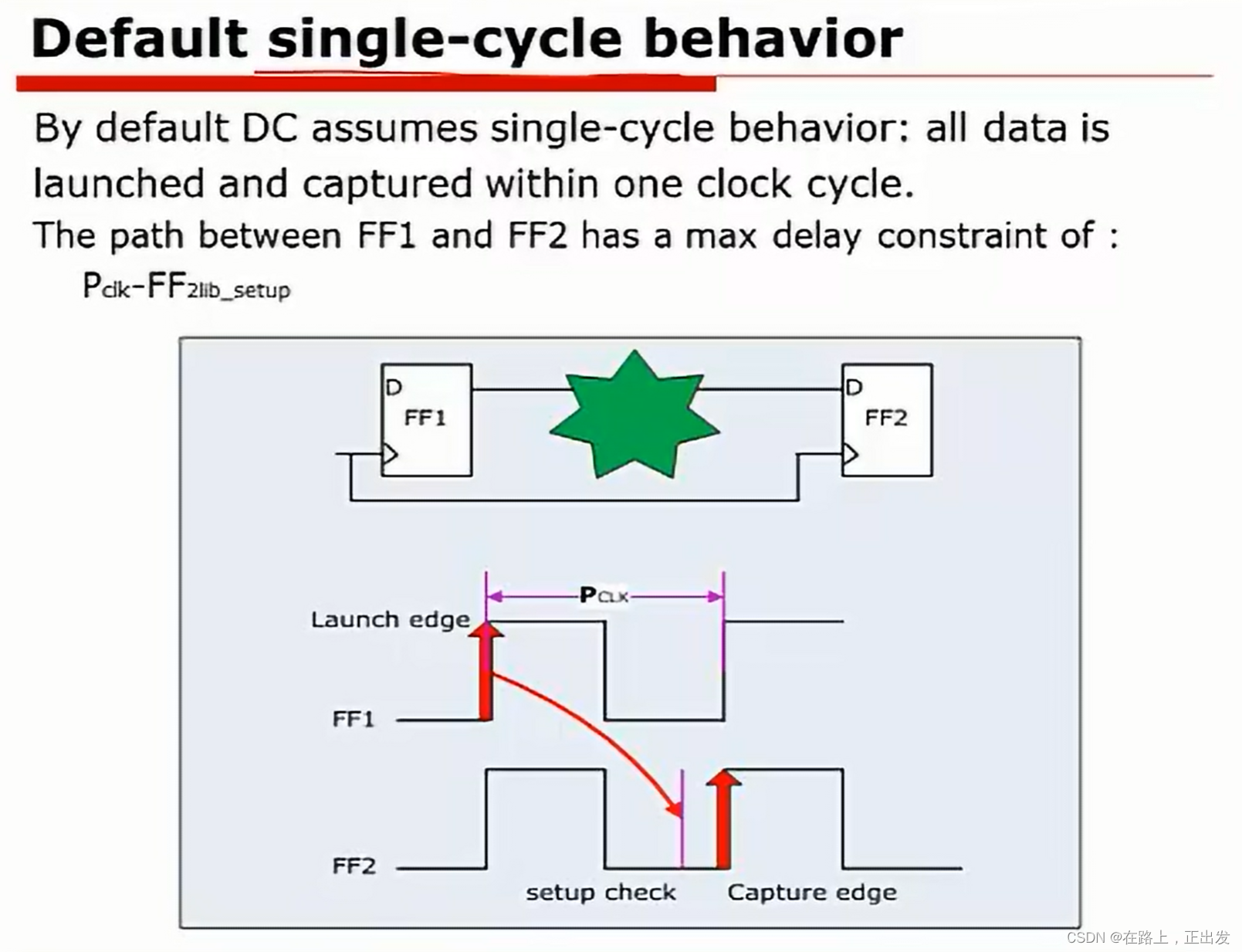
小数点精度位数一般为 13 (-significant_digits)
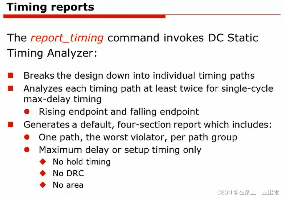
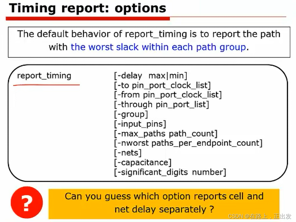
report_timing ::仅报告最差的路径时序;
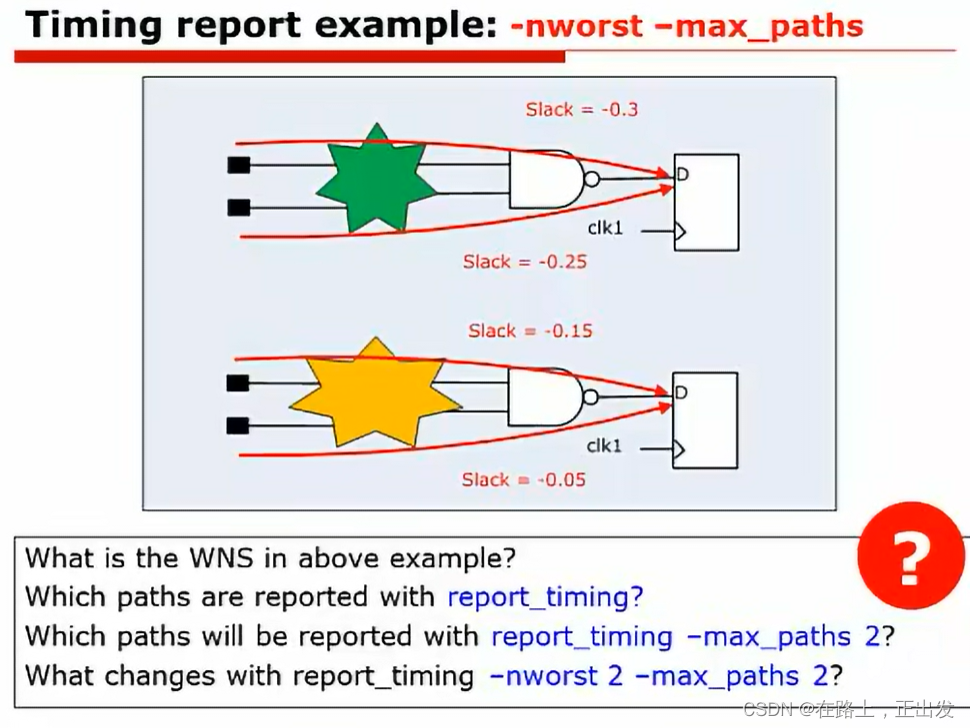
report_timing -max_paths 2 :报告出两条最差的路径,但是这两条路径的终点不同
report_timing -nworst 2 -max_paths 2:报告出整个设计中最差的两条路径,可以是同一个终点
建立时间违规必须全部修改,面积违规和保持时间违规可以保留。
出现违规时可能的情况:输入/出延迟过大,约束过紧;设计的组合逻辑部分延迟过大。


实际操作
以单比特信号以握手方式完成时钟域跨越。
设计源码
// |===================================== TOP ==============================
// |Author:Xu Y. B.
// |Date:2022-11-23
// |Description: TOP module
// |			 about single bit signal CDC using handshake mode
// |			 CDC:100MHz-->50MHz
// |========================================================================module TOP (
// ======================= module input ports specify ==================
// time domain 100MHz
input 						I_CLK_100M,
input 						I_RSTN_100M,// time domain 200MHz
input 						I_CLK_50M,
input 						I_RSTN_50M,// operate enable
input 						I_OPR_EN,//high,start 1 CDC test// ======================= module output ports specify ==================
output 		reg 			O_CDC_DONE);
// ======================= module local parameters =====================// ======================= module internal signals =====================
// register input signal I_OPR_EN
reg 						[1:0]				R_I_OPR_EN;
wire 											W_I_OPR_EN_PDG;
reg 											R_CDC_QST_100M;
reg 						[1:0]				R_CDC_QST_50M;reg 											R_CDC_ACK_50M;
reg 						[1:0]				R_CDC_ACK_100M;// ======================= module design logic =========================
always @ (posedge I_CLK_100M)
begin:pro_opr_en_regif(~I_RSTN_100M)beginR_I_OPR_EN <= 2'b00;endelsebeginR_I_OPR_EN[0] <= I_OPR_EN;R_I_OPR_EN[1] <= R_I_OPR_EN[0];end
endassign W_I_OPR_EN_PDG = R_I_OPR_EN[0] & (~R_I_OPR_EN[1]);always @ (posedge I_CLK_100M)
beginif(~I_RSTN_100M)beginR_CDC_QST_100M <= 0;endelsebeginif(W_I_OPR_EN_PDG)beginR_CDC_QST_100M <= 1;endelse if(R_CDC_ACK_100M[1])beginR_CDC_QST_100M <= 0;endelsebeginR_CDC_QST_100M <= R_CDC_QST_100M;endend
endalways @ (posedge I_CLK_100M)
beginif(~I_RSTN_100M)beginR_CDC_ACK_100M <=2'b0;endelsebeginR_CDC_ACK_100M[0] <= R_CDC_ACK_50M;R_CDC_ACK_100M[1] <= R_CDC_ACK_100M[0];end
end// 50M
always @ (posedge I_CLK_50M)
beginif(~I_RSTN_50M)beginR_CDC_ACK_50M <= 0;endelsebeginif(R_CDC_QST_50M[1])beginR_CDC_ACK_50M <= 1;endelsebeginR_CDC_ACK_50M <= 0;endend
endalways @ (posedge I_CLK_50M)
beginif(~I_RSTN_50M)beginR_CDC_QST_50M <= 2'b00;endelsebeginR_CDC_QST_50M[0] <= R_CDC_QST_100M;R_CDC_QST_50M[1] <= R_CDC_QST_50M[0];end
endalways @ (posedge I_CLK_100M)
beginif(~I_RSTN_100M)beginO_CDC_DONE <= 0;endelsebeginif(R_CDC_ACK_100M)beginO_CDC_DONE <= 1;endelsebeginO_CDC_DONE <= 0;endend
endendmodule
仿真源码
// |========================== Test Bench ===========================
// |Author:Xu Y. B.
// |Date:2022-11-23
// |Description: TOP module
// |			 about single bit signal CDC using handshake mode
// |			 CDC:100MHz-->50MHz
// |			 Test Bench
// |==================================================================module TB ();// time domain 100MHz
reg 						I_CLK_100M;
reg 						I_RSTN_100M;// time domain 200MHz
reg 						I_CLK_50M;
reg 						I_RSTN_50M;// operate enable
reg 						I_OPR_EN;//high,start 1 CDC test// ======================= module output ports specify ==================
wire			 			O_CDC_DONE;// ======================= generate clocks ==============================
initial I_CLK_100M = 0;
always #5 I_CLK_100M = ~I_CLK_100M;initial I_CLK_50M = 0;
always #10 I_CLK_50M = ~I_CLK_50M;initial
beginI_RSTN_100M = 0;I_RSTN_50M = 0;I_OPR_EN = 0;#20;I_RSTN_100M = 1;#40;I_RSTN_50M = 1;#20;I_OPR_EN = 1;@(negedge O_CDC_DONE)#50;$finish;
endinitial
begin`ifdef VPD_TEST$vcdpluson();`endif
endTOP INST_TOP(.I_CLK_100M  (I_CLK_100M),.I_RSTN_100M (I_RSTN_100M),.I_CLK_50M   (I_CLK_50M),.I_RSTN_50M  (I_RSTN_50M),.I_OPR_EN    (I_OPR_EN),.O_CDC_DONE  (O_CDC_DONE));endmodule
VCS执行仿真
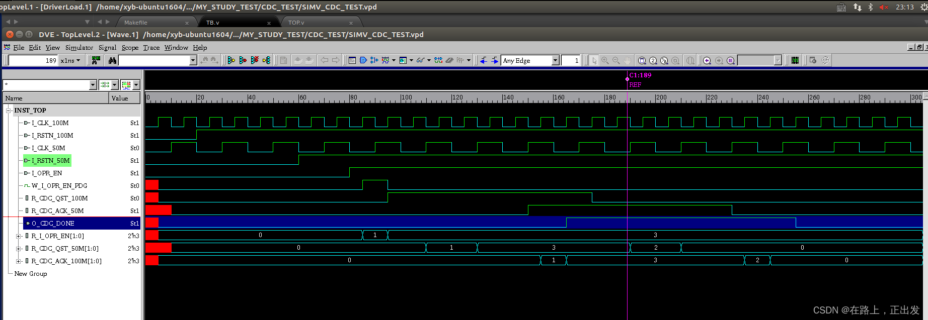
makefile 文件:
# =======================================================
# ========================== MAKE FILE ==================
# By:Xu Y. B.
# Date:2022-11-23
# Note:
# reuse this makefile ,the followings should be changed:
# -1- OUTPUT
# -2- TB file add the following:
# 	  `ifdef VPD_TEST
# 			$vcdpluson();
# 	  `endif
# =======================================================.PHONY: com cov clean debugOUTPUT = SIMV_CDC_TESTVPD_SW_DEFINE = +define+VPD_TEST# code coverage command
CM = -cm line+cond+fsm+branch+tgl
CM_NAME = -cm_name $(OUTPUT)
CM_DIR = -cm_dir ./$(OUTPUT).vdb# vpdfile name
VPD_NAME = $(OUTPUT).vpd# compile command
VCS = vcs -full64 -cpp g++-4.8 -cc gcc-4.8 -LDFLAGS -Wl,--no-as-needed   \-simprofile 							 \-sverilog +v2k -timescale=1ns/1ns      \-debug_access+r 	             		 \-Mupdate								 \+notimingcheck			     		 \+nospecify			                 \+vcs+flush+all			             \$(VPD_SW_DEFINE)						 \-o $(OUTPUT)							 \-l compile.log						 # $(CM)				                 	 \# $(CM_NAME)							 \# $(CM_DIR)
# -cm_hier ./vcs_cov.cfg# simulation command
SIM = ./$(OUTPUT)							 \-l $(OUTPUT).log						 \$(CM) $(CM_NAME) $(CM_DIR)	         \$(VPD_NAME)							 \# start complie
com:	find -name "*.v" >filelist.f $(VCS) -f filelist.f# start simulation
sim:$(SIM)mv vcdplus.vpd $(VPD_NAME)# show the coverage
cov:dve -full64 -covdir *.vdb &
debug:dve -full64 -vpd $(OUTPUT).vpd &# start clean
clean:rm -rf ./csrc *.daidir *.log *.vpd *.vdb simv* *.key *race.out* *.so.* *profile* *.f
DC 综合
脚本:
供参考~~~~~~~~~~
# |===========================================================
# | Author 		: Xu Y. B.
# | Date   		: 2022-11-21
# | Description : tcl script for top design
# |===========================================================# |===========================================================
# |STEP 1: Read & elaborate the RTL design file list & check
# |===========================================================
set TOP_MODULE CDC_TOP
analyze        -format verilog [list CDC_TOP.v ]
elaborate      $TOP_MODULE     -architecture verilog
current_design $TOP_MODULEif {[link] == 0} {echo "Your Link has errors !";exit;
}if {[check_design] == 0} {echo "Your check design has errors !";exit;
}# |===========================================================
# |STEP 2: reset design
# |===========================================================
reset_design# |===========================================================
# |STEP 3: Write unmapped ddc file
# |===========================================================
uniquify
set uniquify_naming_style "%s_%d"
write -f ddc -hierarchy -output ${UNMAPPED_PATH}/${TOP_MODULE}.ddc# |===========================================================
# |STEP 4: define clocks
# |===========================================================
# -------------------------- CLK 100MHz ----------------------
set       CLK_NAME          	I_CLK_100M
set       CLK_PERIOD        	10
set       CLK_SKEW	        	[expr {$CLK_PERIOD*0.05}]
set       CLK_TRANS         	[expr {$CLK_PERIOD*0.01}]
set       CLK_SRC_LATENCY   	[expr {$CLK_PERIOD*0.1 }]
set       CLK_LATENCY       	[expr {$CLK_PERIOD*0.1 }]						create_clock 			-period 	$CLK_PERIOD  	  [get_ports $CLK_NAME]
set_ideal_network 						 			  [get_ports $CLK_NAME]
set_dont_touch_network 					 			  [get_ports $CLK_NAME]
set_drive 				0 							  [get_ports $CLK_NAME]set_clock_uncertainty   -setup       $CLK_SKEW        [get_clocks $CLK_NAME]
set_clock_transition    -max         $CLK_TRANS       [get_clocks $CLK_NAME]
set_clock_latency       -source -max $CLK_SRC_LATENCY [get_clocks $CLK_NAME]
set_clock_latency       -max         $CLK_LATENCY     [get_clocks $CLK_NAME]# --------------------------- CLK 50MHz ----------------------
set       CLK_NAME_2          	I_CLK_50M
set       CLK_PERIOD_2        	20
set       CLK_SKEW_2	        [expr {$CLK_PERIOD_2*0.05}]
set       CLK_TRANS_2         	[expr {$CLK_PERIOD_2*0.01}]
set       CLK_SRC_LATENCY_2   	[expr {$CLK_PERIOD_2*0.1 }]
set       CLK_LATENCY_2       	[expr {$CLK_PERIOD_2*0.1 }]						create_clock 			-period 	$CLK_PERIOD_2  	  [get_ports $CLK_NAME_2]
set_ideal_network 						 			  [get_ports $CLK_NAME_2]
set_dont_touch_network 					 			  [get_ports $CLK_NAME_2]
set_drive 				0 							  [get_ports $CLK_NAME_2]set_clock_uncertainty   -setup       $CLK_SKEW_2        [get_clocks $CLK_NAME_2]
set_clock_transition    -max         $CLK_TRANS_2       [get_clocks $CLK_NAME_2]
set_clock_latency       -source -max $CLK_SRC_LATENCY_2 [get_clocks $CLK_NAME_2]
set_clock_latency       -max         $CLK_LATENCY_2     [get_clocks $CLK_NAME_2]# |===========================================================
# |STEP 5: define reset
# |===========================================================
# ------------------------- RST 1 ----------------------------
set RST_NAME 					I_RSTN_100M
set_ideal_network 				[get_ports $RST_NAME]
set_dont_touch_network          [get_ports $RST_NAME]
set_drive             0         [get_ports $RST_NAME]# ------------------------- RST 2 ----------------------------
set RST_NAME_2 					I_RSTN_50M
set_ideal_network 				[get_ports $RST_NAME_2]
set_dont_touch_network          [get_ports $RST_NAME_2]
set_drive             0         [get_ports $RST_NAME_2]# |===========================================================
# |STEP 6: set input delay using timing budget
# |Assume a weak cell to drive the input pins
# |===========================================================
set 		LIB_NAME 			typical
set 		WIRE_LOAD_MODEL 	smic18_wl10
set 		DRIVE_CELL 			INVX1
set 		DRIVE_CELL_2 		INVX4
set 		DRIVE_CELL_3		INVX8set 		DRIVE_PIN 			Y
set 		OPERATE_CONDITION   typicalset 		INPUT_RST 			 [get_ports I_RSTN_100M]
set 		INPUT_RST_2			 [get_ports I_RSTN_50M]set         INPUT_DELAY 		 [expr {$CLK_PERIOD*0.6}]
set         INPUT_DELAY_2 		 [expr {$CLK_PERIOD_2*0.6}]
# CLK 1
set_input_delay $INPUT_DELAY -clock $CLK_NAME [get_ports I_OPR_EN]
set_input_delay $INPUT_DELAY -clock $CLK_NAME ${INPUT_RST}# CLK 2
set_input_delay $INPUT_DELAY_2 -clock $CLK_NAME_2 ${INPUT_RST_2}# DRIVE CELL
set_driving_cell -lib_cell ${DRIVE_CELL}   -pin ${DRIVE_PIN}   ${INPUT_RST}
set_driving_cell -lib_cell ${DRIVE_CELL_2} -pin ${DRIVE_PIN}   ${INPUT_RST_2}
set_driving_cell -lib_cell ${DRIVE_CELL_3} -pin ${DRIVE_PIN}   [get_ports I_OPR_EN]# |===========================================================
# |STEP 7: set output delay
# |===========================================================
set OUTPUT_DELAY  [expr {$CLK_PERIOD*0.6}]
set MAX_LOAD      [expr {[load_of $LIB_NAME/INVX4/A] * 10}]set_output_delay  $OUTPUT_DELAY -clock $CLK_NAME 	 [all_outputs]
set_load 		  [expr {$MAX_LOAD * 3}] 			 [all_outputs]
set_isolate_ports -type buffer 					 	 [all_outputs]# |===========================================================
# |STEP 8: set max delay for comb logic
# |===========================================================
# set_input_delay  [expr $CLK_PERIOD * 0.1] -clock $CLK_NAME -add_delay [get_ports I_1]
# set_output_delay [expr $CLK_PERIOD * 0.1] -clock $CLK_NAME -add_delay [get_ports O_1]# |===========================================================
# |STEP 9: set operating condition & wire load model
# |===========================================================
set_operating_conditions -max 			$OPERATE_CONDITION \-max_library 	$LIB_NAMEset 					 auto_wire_load_selection false
set_wire_load_mode  	 top
set_wire_load_model		 -name    $WIRE_LOAD_MODEL \-library $LIB_NAME# |===========================================================
# |STEP 10: set area constraint (Let DC try its best)
# |===========================================================
set_max_area			 1000# |===========================================================
# |STEP 11: set DRC constraint
# |===========================================================
# set MAX_CAPACITANCE [expr {[load_of $LIB_NAME/NAND4X2/Y] * 5}]
# set_max_capacitance $MAX_CAPACITANCE $ALL_INPUT_EXCEPT_CLK# |===========================================================
# |STEP 12: set group path
# |Avoid getting stack on one path
# |===========================================================
# group_path -name $CLK_NAME -weight 5 				\
# 						   -critical_range  [expr {$CLK_PERIOD * 0.1}] # group_path -name INPUTS    -from [all_inputs] 		\
# 					 	   -critical_range  [expr {$CLK_PERIOD * 0.1}] # group_path -name OUTPUTS   -to [all_outputs] 		\
# 						   -critical_range  [expr {$CLK_PERIOD * 0.1}] # group_path -name COMBS     -from [all_inputs] 		\
# 						   -to [all_outputs] 		\
# 						   -critical_range  [expr {$CLK_PERIOD * 0.1}]
# report_path_group# |===========================================================
# |STEP 13: Elimate the multiple-port inter-connect &
# |			define name style
# |===========================================================
# set_app_var 						verilogout_no_tri 					true
# set_app_var						verilogout_show_unconnected_pins 	true
# set_app_var						bus_naming_style					{%s[%d]}
# simplify_constants 				-boundary_optimization
# set_boundary_optimization 		[current_design] 					true
# set_fix_multiple_port_nets 		-all 								-buffer_constants# |===========================================================
# |STEP 14: timing exception define
# |===========================================================
# set_false_path -from [get_clocks I_CLK_100M] -to [get_clocks I_CLK_100M]
# set ALL_CLKS [all_clocks]
# foreach_in_collection CUR_CLK $ALL_CLKS
# {
# 	set OTHER_CLKS [remove_from_collection [all_clocks] $CUR_CLK]
# 	set_false_path -from $CUR_CLK $OTHER_CLKS
# }# set_false_path -from [get_clocks I_CLK_100M] -to [get_clocks I_CLK_100M]
# set_false_path -from [get_clocks I_CLK_100M] -to [get_clocks I_CLK_100M]# set_disable_timing TOP/U1 -from a -to y
# set_case_analysis 0 [get_ports sel_i]# set_multicycle_path -setup 6 -from FFA/CP -through ADD/out -to FFB/D
# set_multicycle_path -hold 5 -from FFA/CP -through ADD/out -to FFB/D
# set_multicycle_path -setup 2 -to FFB/D
# set_multicycle_path -hold 1 -to FFB/D# |===========================================================
# |STEP 15: compile flow
# |===========================================================
# ungroup -flatten -all# 1st-pass compile
# compile -map_effort high -area_effort high
# compile -map_effort high -area_effort high -boundary_optimization
compile # simplify_constants -boundary_optimization
# set_fix_multiple_port_nets -all -buffer_constants# compile -map_effort high -area_effort high -incremental_mapping -scan# 2nd-pass compile
# compile -map_effort high -area_effort high -incremental_mapping -boundary_optimization
# compile_ultra -incr# |===========================================================
# |STEP 16: write post-process files
# |===========================================================
# change_names -rules verilog -hierarchy
# remove-unconnected_ports [get_cells -hier *] -blast_buses
# Write the mapped files
write -f ddc -hierarchy -output $MAPPED_PATH/${TOP_MODULE}.ddc
# write 	-f verilog 	-hierarchy -output 	$MAPPED_PATH/${TOP_MODULE}.v
# write_sdc -version 	1.7 				$MAPPED_PATH/${TOP_MODULE}.sdc
# write_sdf -version 	2.1 				$MAPPED_PATH/${TOP_MODULE}.sdf# |===========================================================
# |STEP 17: generate report files
# |===========================================================
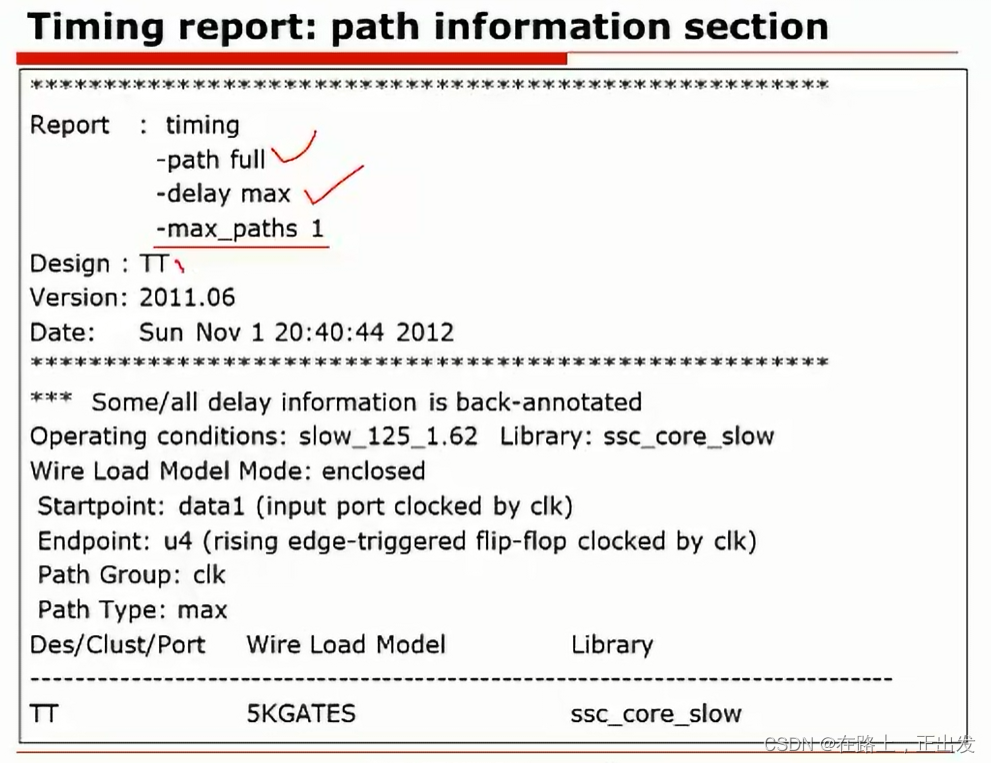
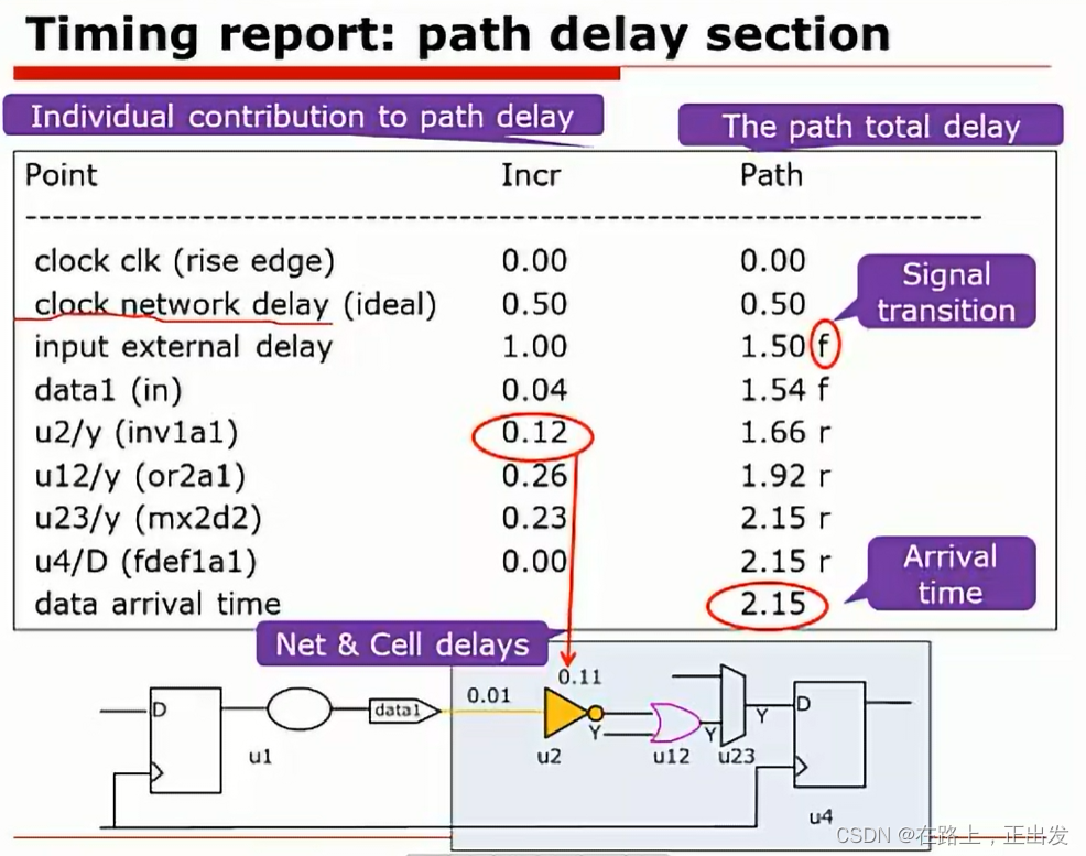
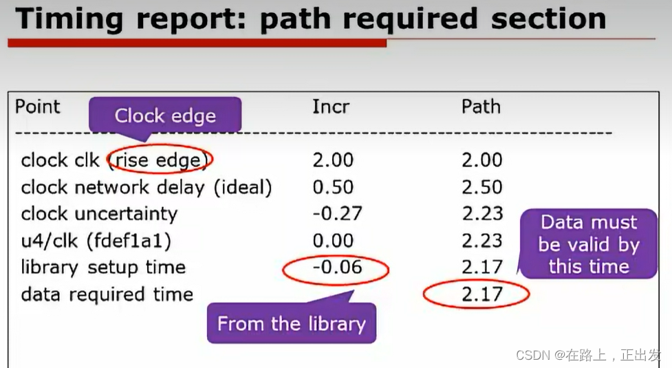
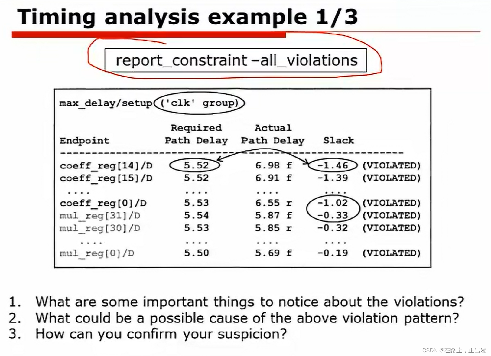
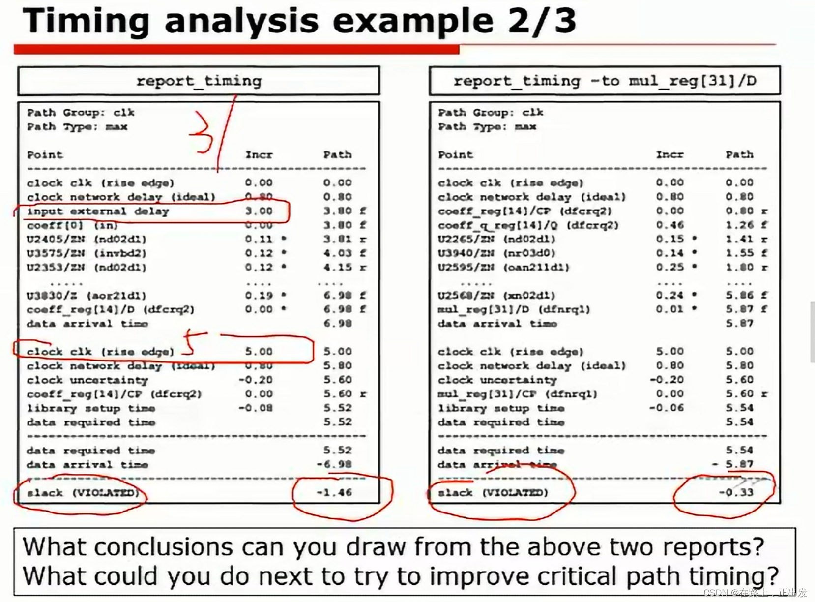
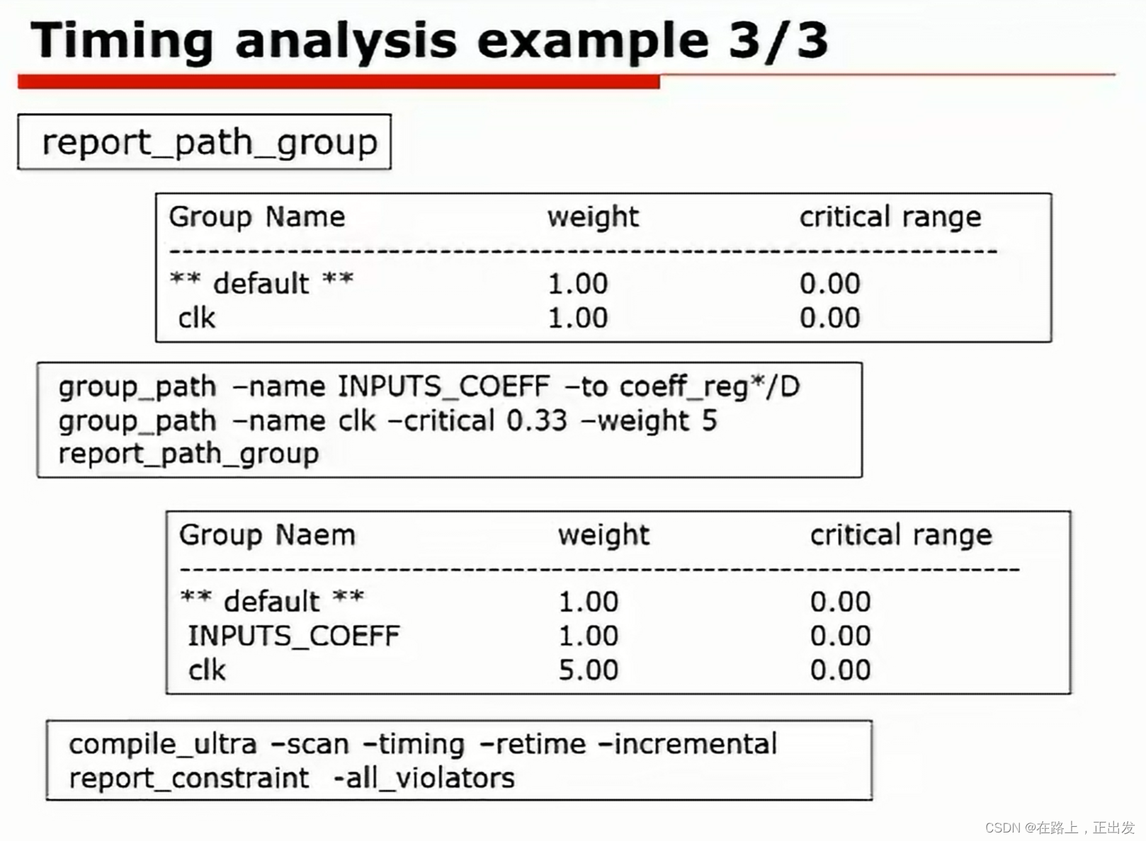
在完成编译之后可以用本篇的PPT里面介绍的 时序报告指令进行时序分析。此处不再赘述。


![[ Linux ] 进程间通信之共享内存](https://img-blog.csdnimg.cn/img_convert/adb91f1dfacd7779e7828fe68029fea4.png)